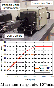
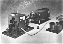
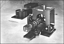
PEMI II is used to measure in-plane deformations of semiconductor packages. Flat surface of the specimen is replicated with diffraction grating of 2400 lines/mm, and is subjected to thermal or mechanical loading.
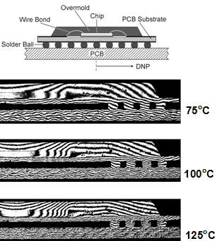
Example: Thermal deformations of WB-PBGA package assembly